Imagine
!!
  People   Project   Publications   More Info  
    architecture   programming   performance   VLSI   board   applications   tools  


Imagine VLSI Implementation


Implementation Overview

On April 9th, 2002, first samples of a prototype Imagine stream processor were received at Stanford. A wafer containing 93 Imagine die is shown to the left. (Click on the picture for a larger view).

The Imagine stream processor is a 16mm x 16mm, 21 million transistor chip implemented by a collaboration between Stanford Unversity and Texas Instruments (TI) in a 1.5V 0.15 micron process with five layers of aluminum metal. Stanford designed the architecture, logic, and did the floorplanning and cell placement. TI completed the layout and layout verification.

Building a prototype Imagine processor contributed in three key ways to the overall project. First, many things were learned about the stream architecture by implementing Imagine in VLSI. Second, having prototype processors available enables real-time application and tool development which is not possible on hardware simulators. Finally, building a prototype Imagine provides a proof-of-concept to the VLSI feasibility of the processor and allows architectural studies to be based on results from actual silicon.

 

Schedule

The Imagine implementation effort began in autumn, 1998. At its peak, the Stanford team working on design and verification six graduate students working on design and verification. The history of the Imagine implementation is shown below. In total, Stanford expended 11 person-years of work on the logic design, floorplanning, and placement of the Imagine processor.

  • 11/1998: Logic design commenced (team consists of one student writing the behavioral RTL for an ALU cluster)
  • 11/2000: First trial placement of an ALU cluster completed
  • 12/2000: Behavioral RTL completed and functionally verified (team has grown to five graduate students)
  • 08/2001: Final placement and floorplanning completed by Stanford, and design is handed off to TI for layout and layout verification
  • 02/2002: Imagine parts enter a TI fab (part number F741749)
  • 04/2002: Stanford receives Imagine parts
  • 06/2002: First full application succesfully run in the lab


Design Methodology

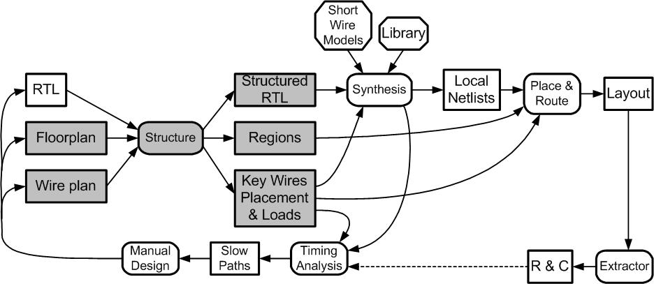
Imagine was designed in a standard cell technology using the TI-ASIC design methodology. Detailed information on the design methodology can be found in "VLSI Design and Verification of the Imagine Processor"

A graphical representation of the Imagine tool flow is shown above. RTL was written in Verilog and mapped to the standard-cell library with Synopsys Design Compiler. Datapath-style placement of standard cells was carried out using a tiled-region design methodology. Tiled regions allowed for hand-assisted automatic placement of key standard cells in datapath bitslices. This methodology provided a good compromise between design effort and performance. The Avant! Apollo tool suite was used for placement, routing, and clock distribution.


Die Photo

The final cell placement and die photo of the Imagine chip are shown below.

Figure 1. Final cell placement of Imagine (click image for larger view)

Figure 2. Die Photo of Imagine (click image for larger view)


gajh@cva.stanford.edu